
From crystal to component
A clear route from material to part.
Six stages take you from choosing a crystal to inspecting a finished component. Each project sets its own route.
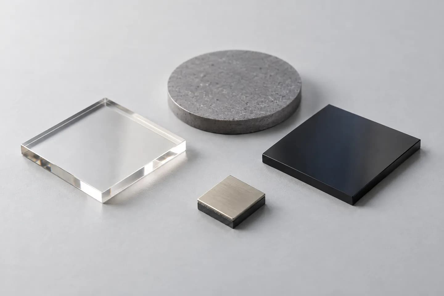
Material Selection
You decide the crystal type, grade and which property matters most.
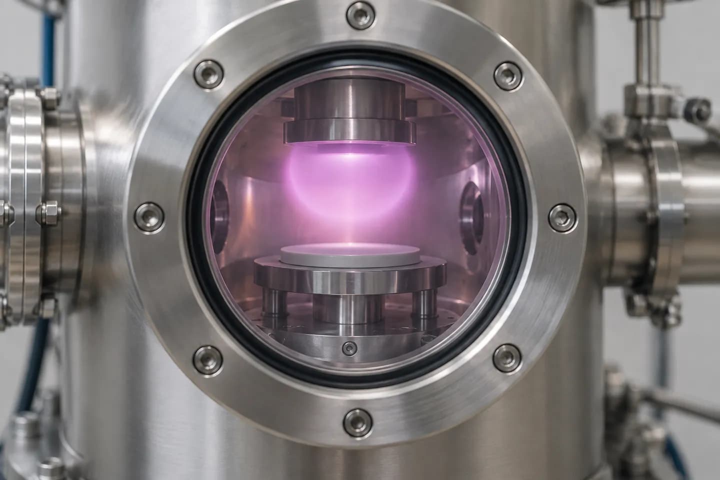
Diamond Growth
You set the growth route, purity and doping your application needs.
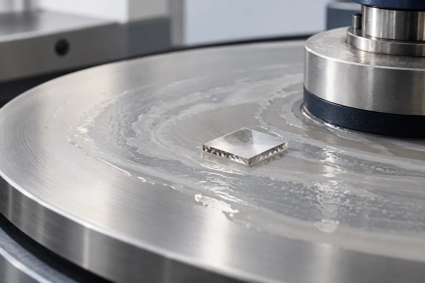
Precision Processing
You get a dimensioned drawing with tolerances and surface finish agreed.
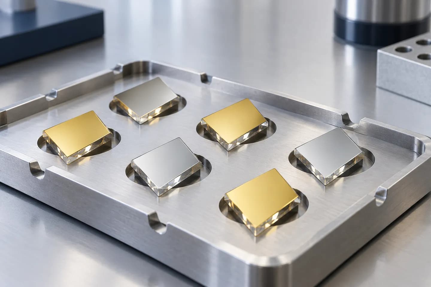
Surface Engineering
You define the surface condition, plus any metal layers or patterns.
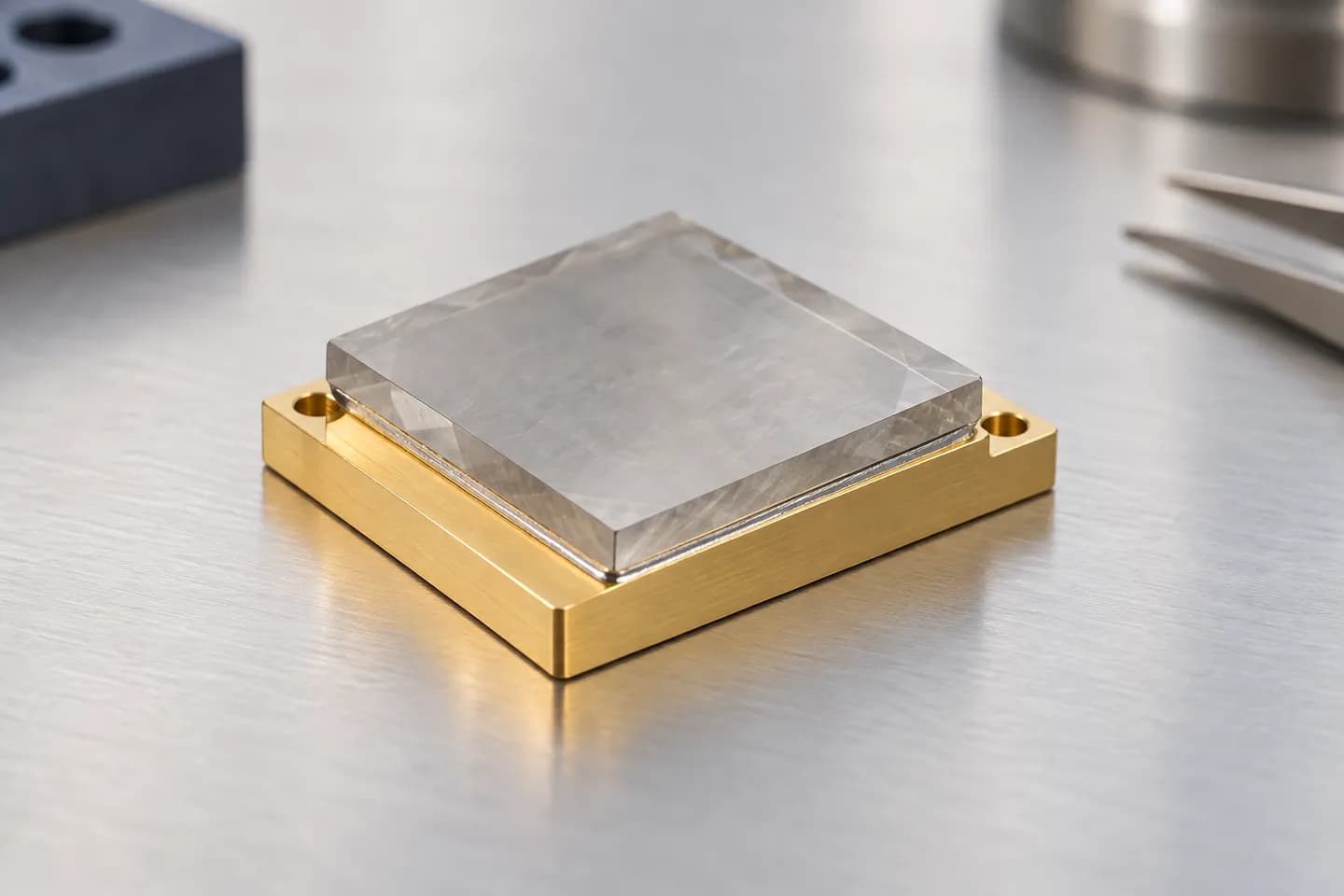
Integration
You agree the assembly stack and how the interface will be accepted.
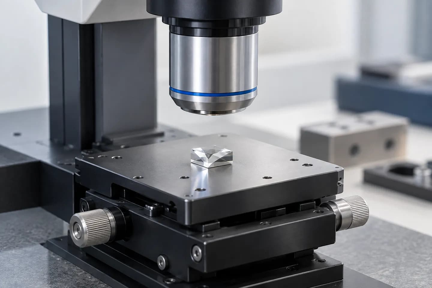
Inspection & Testing
You agree the inspection plan and test records before qualification.
Each project defines its own processing route and inspection plan. These stages describe the engineering workflow; equipment ownership and in-house capability are not implied. Images are representative.
India’s semiconductor vision
An ecosystem built together.
The SEMICON India 2026 address highlighted materials, equipment, research and domestic supply chains as parts of a connected semiconductor ecosystem.
Source: SEMICON India address · 17 September 2026
Read the official address (opens in a new tab)Industry context. No government affiliation or endorsement of ADAMYX is implied.
Requirement to review
Define the next step. Together.
Bring the application, the constraints and the outcome you need. We’ll help scope the engineering review.