
Product family
Integrated & Bonded Substrates Connect diamond to your device
For teams building diamond into a device stack, with bonded, grown or clad layers and a defined interface.
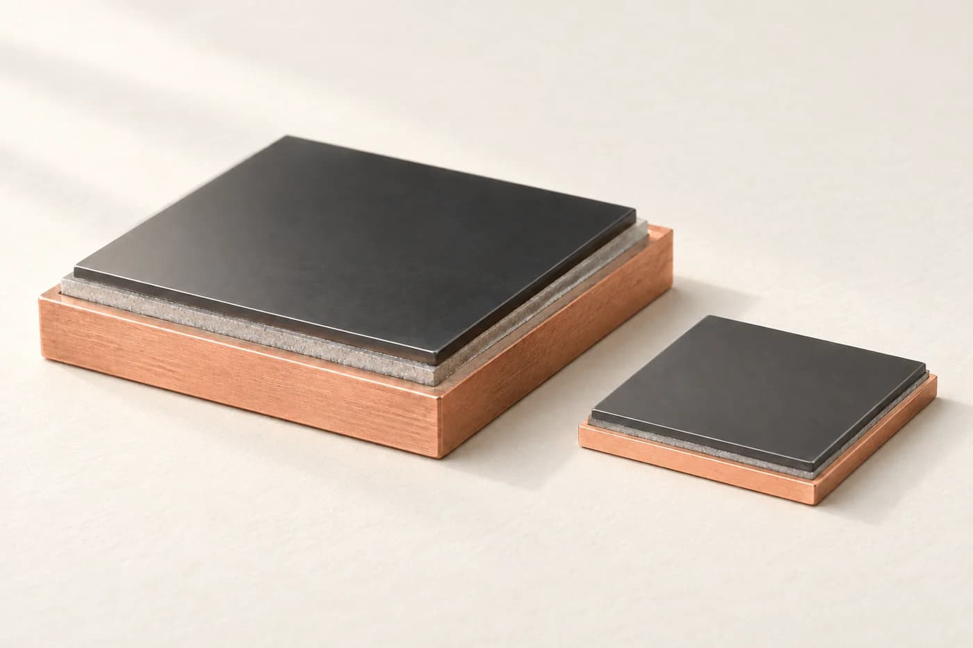
Ways to integrate diamond
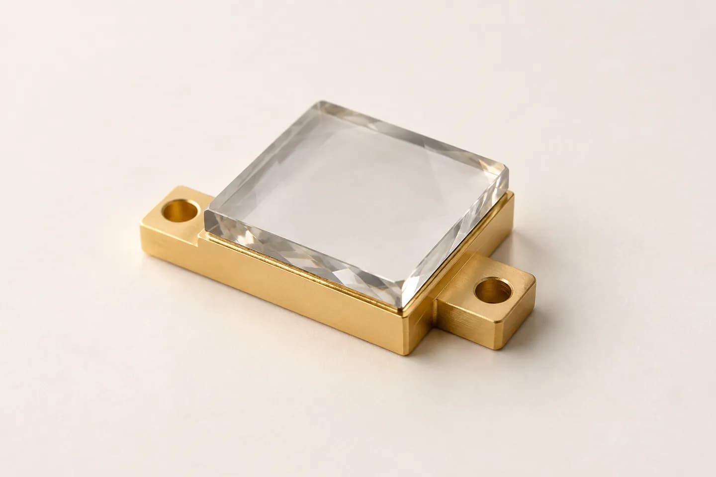
Custom Bonded Diamond Assemblies
Diamond joined to another material as part of your device or thermal stack.
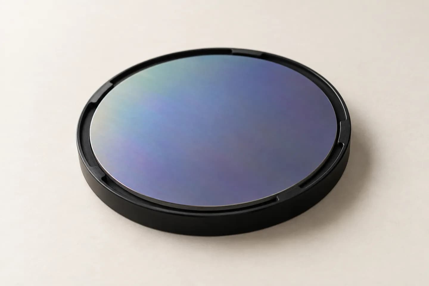
GaN-on-Diamond
Brings gallium nitride (GaN) close to a diamond layer that conducts heat.
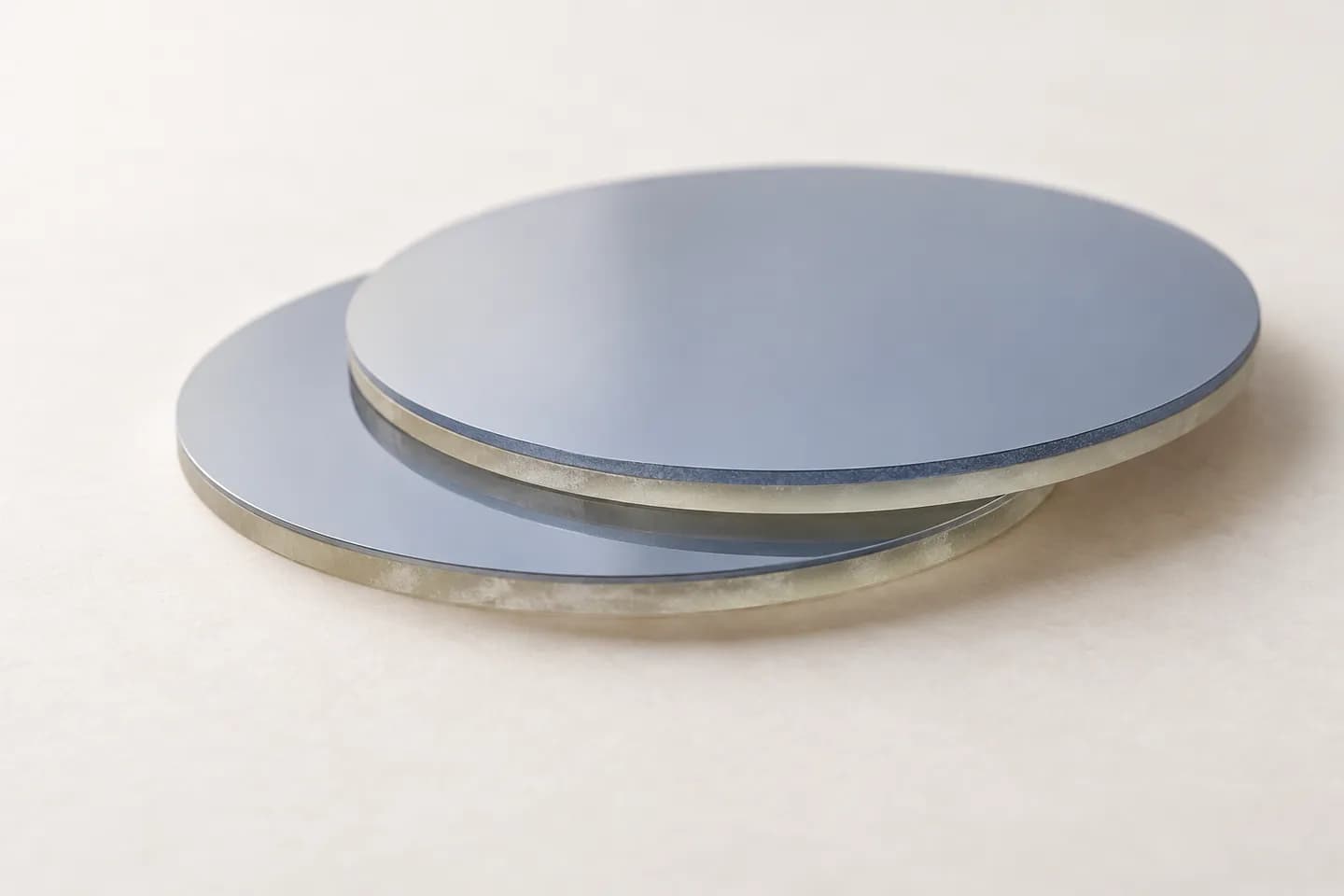
GaN Bonded to Diamond Wafers
GaN joined to diamond by bonding or layer transfer.
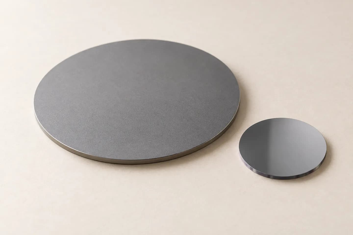
Diamond-on-Silicon
A diamond layer carried on silicon rather than a free-standing diamond part.
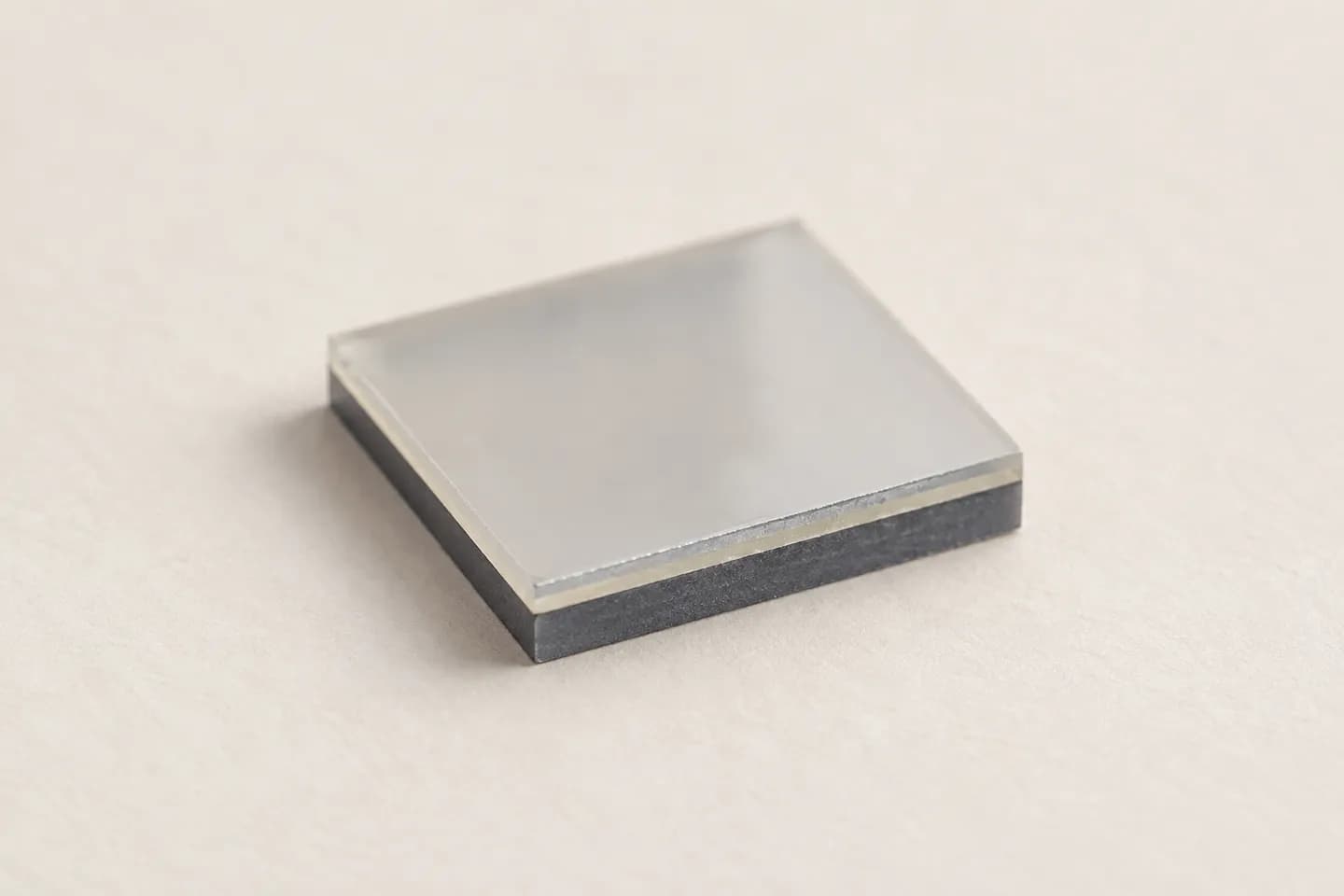
Diamond-on-Oxide / Insulator
Diamond over an insulating oxide for structures that need a distinct support.
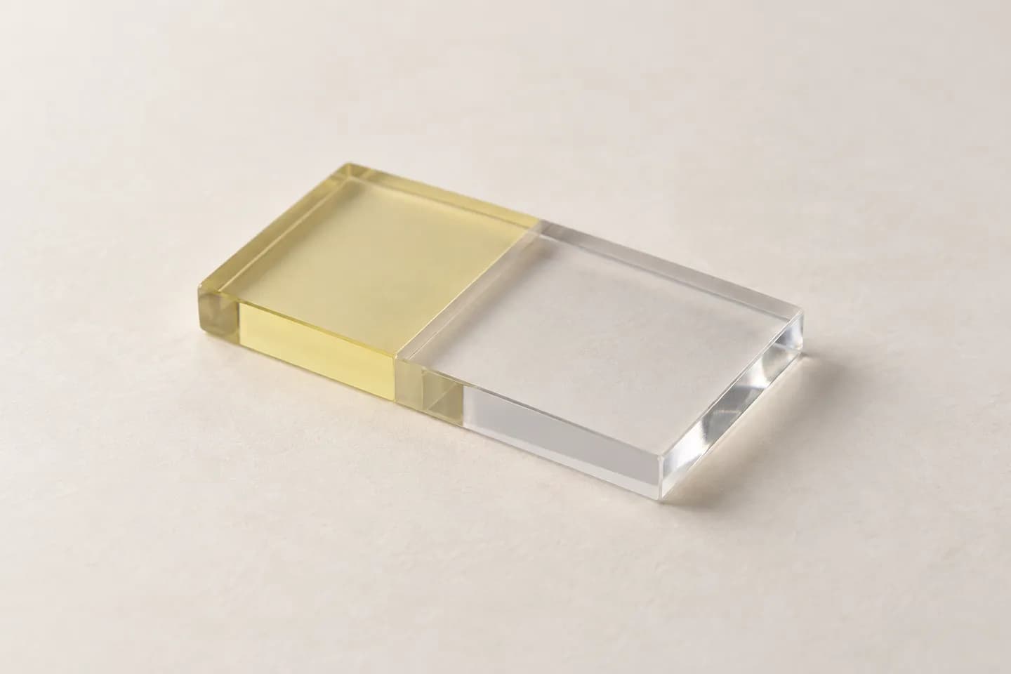
Diamond–Yb:YAG Bonded Substrates
Joins diamond to Yb:YAG to give a laser crystal a thermal path.
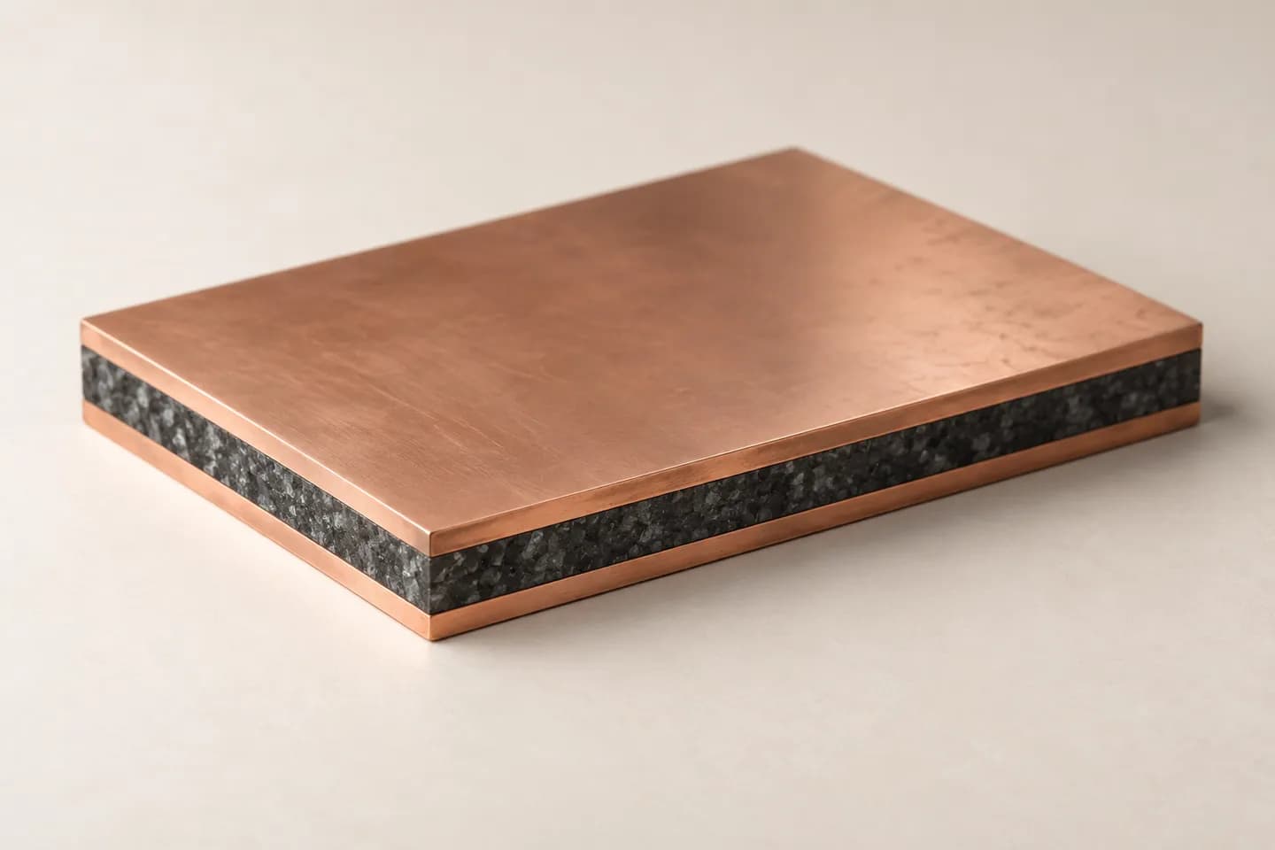
Copper-Clad CVD Diamond
CVD diamond laminated with copper layers to form a thermal component.
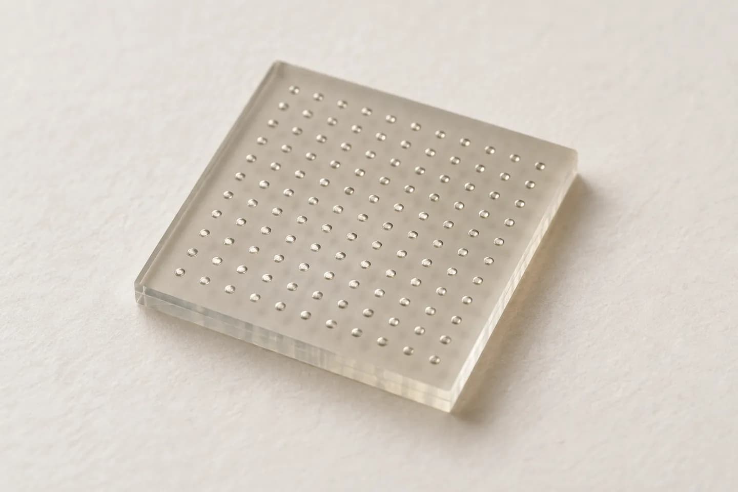
Through-Diamond Via Substrates
Diamond substrates with through-thickness features for an integrated package.
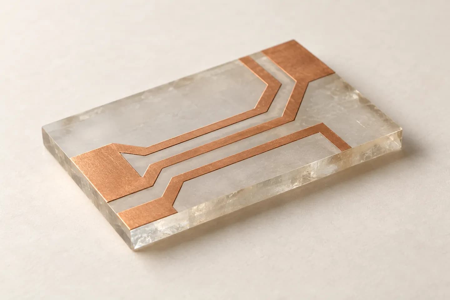
Direct-Bonded Copper on Diamond
Copper bonded directly to diamond for thermal and electrical integration.

Strain-Balanced Diamond Substrates
Layered substrates arranged to manage deformation caused by thermal expansion.
Product images are representative.
What we will ask you
Bring what you know. We confirm the details with you during technical review.
- What layers make up your stack?Materials, layer order and thicknesses.
- How must the interface perform?Bonding or joining method and your interface acceptance criteria.
- What wafer size and conditions apply?Wafer or part size, operating temperature and environment.
Full specification checklist for engineers
Dimensions & tolerances
- Lateral size, outline or diameter, and tolerancemm
- Thickness and tolerance (bulk or layer)mm
- Flatness or surface figure, and bowµm or fringes
- Via diameter and pitchµm
Surface & finish
- Surface roughness per sidenm Ra
Material properties
- Coefficient of thermal expansion (per temperature range)ppm/K
Metallization & joining
- Layer sequence and thicknesses (including interlayers)µm
- Bond integrity and bonded area%
- Process temperature budget and thermal cycling°C
- Interface absorption lossppm
- Metallization or plating stack and thicknessnm per layer
- Metallization pattern and coverage
Optical performance
- Coating construction and thicknessnm
Electrical & electrochemical
- Electrical isolationΩ
Integration & packaging
- Thermal boundary resistancem²K/W
- Substrate, carrier or diamond form
- Wafer bow and warp (including over temperature)µm
- Partner crystal dopant, orientation and geometry
Common questions
All questionsAre these stock wafers?
No. These are integration routes reviewed project by project. Feasibility and supply scope are established for your proposed stack before any commitment.
What do you need to review a bonded stack?
Layer sequence and thicknesses, wafer or coupon size, bonded area, temperature budget and interface requirements. Tell us about bow, isolation and cycling needs as well.
How do I choose between GaN-on-diamond and a bonded route?
GaN-on-diamond brings GaN close to diamond by growth or bonding. Bonded wafers join separately made layers. The choice depends on your device, temperature budget and interface needs, reviewed in technical review.
Requirement to review
Have a material requirement? Let’s review it.
Share your integrated & bonded substrates requirement, dimensions and drawing for review.