
Integrated & Bonded Substrates Supported diamond films
Diamond-on-Silicon
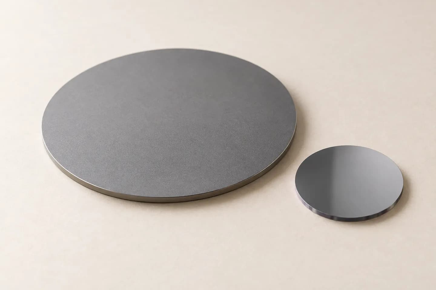
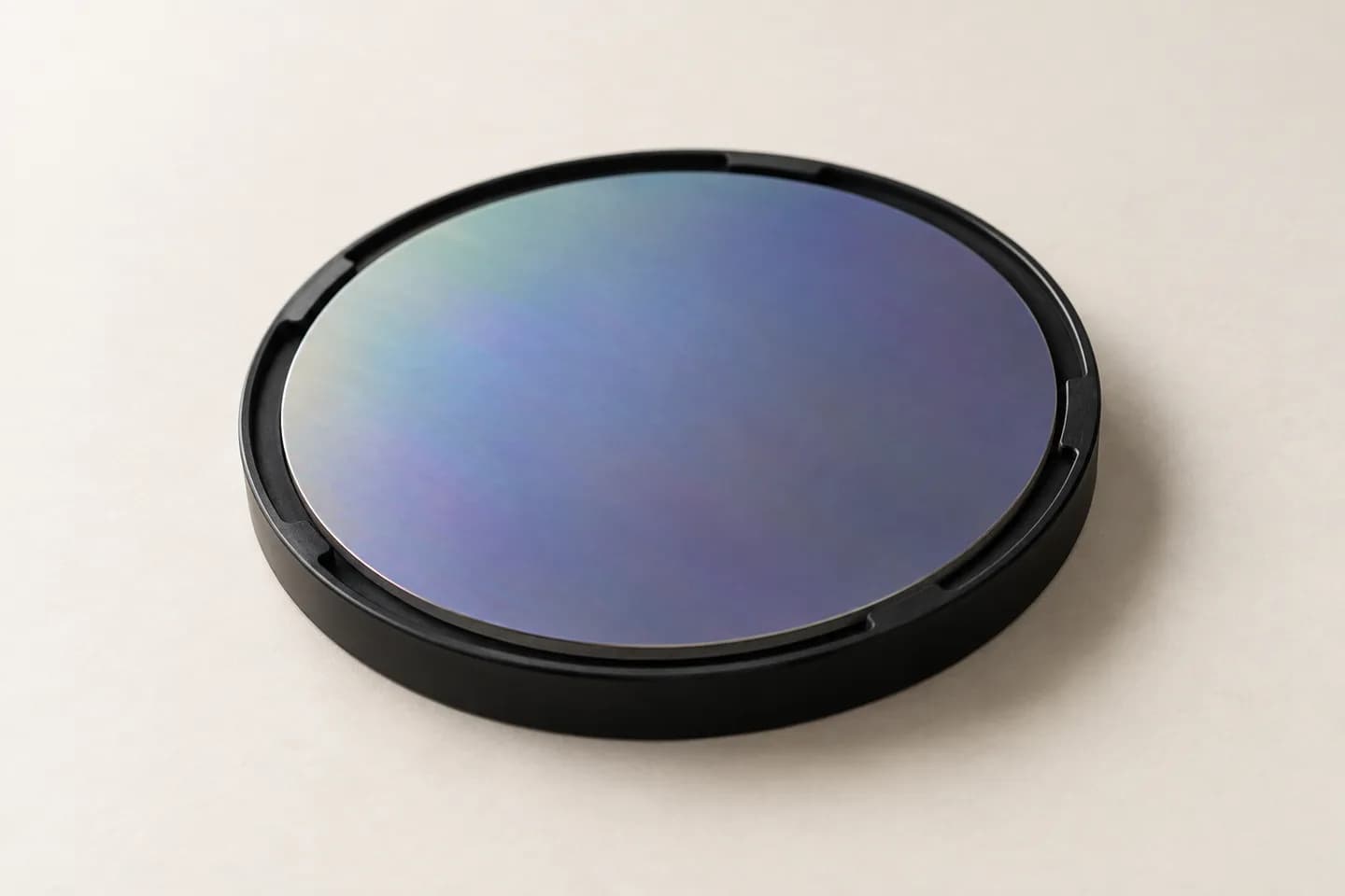
A diamond layer carried on silicon rather than a free-standing diamond part.
Good to know
- The silicon provides support for the diamond layer.
- Diamond thickness and surface condition define the working face.
- Retaining or removing the silicon changes the final component structure.
Specifications
What we define for diamond-on-silicon, with units and how each is typically measured. We confirm values for your application in technical review.
Request the datasheetLook up a term in the glossaryDimensions & tolerances
| Parameter | Unit | Typical test method |
|---|---|---|
| Thickness and tolerance (bulk or layer) | mm | Micrometer or optical gauge |
| Lateral size, outline or diameter, and tolerance | mm | Optical measurement |
| Thickness uniformity (total thickness variation) | µm | Thickness mapping or interferometry |
| Edge condition and chip limit | Microscopy inspection to drawing |
Crystal & purity
| Parameter | Unit | Typical test method |
|---|---|---|
| Grain size and texture | µm | EBSD or optical microscopy |
Surface & finish
| Parameter | Unit | Typical test method |
|---|---|---|
| Surface roughness per side | nm Ra | Profilometry or AFM |
| Surface finish condition (as-grown, lapped or polished) | Visual inspection to drawing |
Material properties
| Parameter | Unit | Typical test method |
|---|---|---|
| Residual stress | MPa | Raman spectroscopy or wafer-curvature method |
| Thermal conductivity grade | W/m·K | Laser flash (ASTM E1461) |
Metallization & joining
| Parameter | Unit | Typical test method |
|---|---|---|
| Layer sequence and thicknesses (including interlayers) | µm | Cross-section microscopy or per drawing |
| Bond integrity and bonded area | % | Acoustic microscopy |
| Process temperature budget and thermal cycling | °C | Thermal-cycle test with post-test inspection |
Integration & packaging
| Parameter | Unit | Typical test method |
|---|---|---|
| Substrate, carrier or diamond form | Per drawing | |
| Wafer bow and warp (including over temperature) | µm | Wafer geometry gauge or profilometry |
| Certificate of conformance and traceability | Supplier declaration |
Where it is used
- Computing & Data CentresDense heat and tight package space need a short path to cooling; diamond spreads it.
- Telecom, RF & RadarRF power raises junction temperature; diamond helps carry heat away while interfaces stay reliable.
- Power Electronics & EVsTemperature cycling demands expansion balance and isolation; diamond components help manage the heat.
- Semiconductor EquipmentProcessing demands precision, cleanliness and compatible materials; diamond parts are specified around all three.
Requirement to review
Have a material requirement? Let’s review it.
Share your diamond-on-silicon requirement, dimensions and drawing for review.