
Integrated & Bonded Substrates Wafer bonding route
GaN Bonded to Diamond Wafers
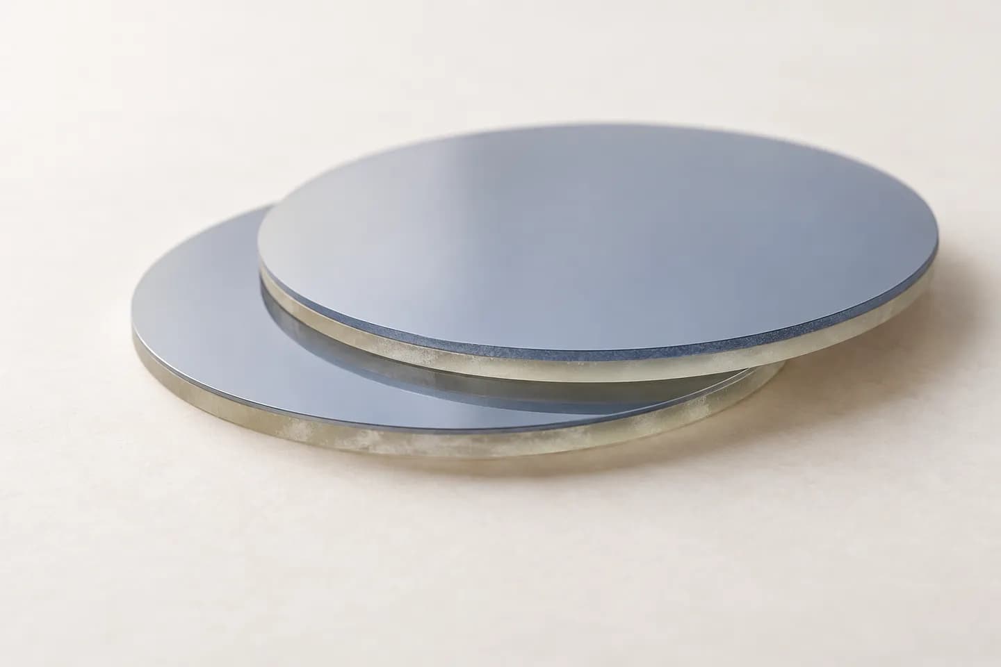
GaN joined to diamond by bonding or layer transfer.
Good to know
- The bond interface is distinct from the GaN and diamond bulk materials.
- Wafer bow, usable area and alignment influence subsequent fabrication.
- Process temperature must be compatible with any existing device structures.
Specifications
What we define for GaN bonded to diamond wafers, with units and how each is typically measured. We confirm values for your application in technical review.
Request the datasheetLook up a term in the glossaryDimensions & tolerances
| Parameter | Unit | Typical test method |
|---|---|---|
| Lateral size, outline or diameter, and tolerance | mm | Optical measurement |
| Thickness and tolerance (bulk or layer) | mm | Micrometer or optical gauge |
| Thickness uniformity (total thickness variation) | µm | Thickness mapping or interferometry |
| Edge condition and chip limit | Microscopy inspection to drawing |
Crystal & purity
| Parameter | Unit | Typical test method |
|---|---|---|
| Crystalline quality (rocking-curve width) | arcsec | XRD rocking curve |
Surface & finish
| Parameter | Unit | Typical test method |
|---|---|---|
| Surface roughness per side | nm Ra | Profilometry or AFM |
Metallization & joining
| Parameter | Unit | Typical test method |
|---|---|---|
| Layer sequence and thicknesses (including interlayers) | µm | Cross-section microscopy or per drawing |
| Bond integrity and bonded area | % | Acoustic microscopy |
| Bonding method and interlayer | Supplier declaration | |
| Process temperature budget and thermal cycling | °C | Thermal-cycle test with post-test inspection |
| Heat-cycle dimensional stability | cycles | Thermal-cycle test with post-test inspection |
Integration & packaging
| Parameter | Unit | Typical test method |
|---|---|---|
| Wafer bow and warp (including over temperature) | µm | Wafer geometry gauge or profilometry |
| Thermal boundary resistance | m²K/W | Time-domain thermoreflectance |
| Certificate of conformance and traceability | Supplier declaration | |
| Inspection plan and documentation | Per drawing |
Where it is used
- Computing & Data CentresDense heat and tight package space need a short path to cooling; diamond spreads it.
- Telecom, RF & RadarRF power raises junction temperature; diamond helps carry heat away while interfaces stay reliable.
- Power Electronics & EVsTemperature cycling demands expansion balance and isolation; diamond components help manage the heat.
- Semiconductor EquipmentProcessing demands precision, cleanliness and compatible materials; diamond parts are specified around all three.

Requirement to review
Have a material requirement? Let’s review it.
Share your GaN bonded to diamond wafers requirement, dimensions and drawing for review.