
Integrated & Bonded Substrates Bonded laser crystals
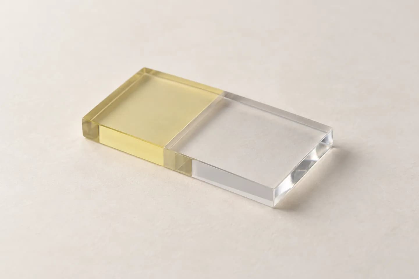
Diamond–Yb:YAG Bonded Substrates
Joins diamond to Yb:YAG to give a laser crystal a thermal path.
Good to know
- Crystal dimensions and bond geometry define the assembly.
- Absorption and distortion at the interface can affect the optical path.
- End-face coatings must match the laser wavelength and cavity design.
Specifications
What we define for diamond–Yb:YAG bonded substrates, with units and how each is typically measured. We confirm values for your application in technical review.
Request the datasheetLook up a term in the glossaryDimensions & tolerances
| Parameter | Unit | Typical test method |
|---|---|---|
| Lateral size, outline or diameter, and tolerance | mm | Optical measurement |
| Flatness or surface figure, and bow | µm or fringes | Interferometry (633 nm) or profilometry |
| Thickness and tolerance (bulk or layer) | mm | Micrometer or optical gauge |
| Parallelism or wedge | arcmin | Autocollimator or interferometry |
| Edge condition and chip limit | Microscopy inspection to drawing |
Surface & finish
| Parameter | Unit | Typical test method |
|---|---|---|
| Surface quality (scratch and dig) | Visual inspection (ISO 10110-7) |
Metallization & joining
| Parameter | Unit | Typical test method |
|---|---|---|
| Interface absorption loss | ppm | Laser calorimetry (ISO 11551) |
| Bond integrity and bonded area | % | Acoustic microscopy |
| Bonding method and interlayer | Supplier declaration |
Optical performance
| Parameter | Unit | Typical test method |
|---|---|---|
| Coating construction and thickness | nm | Spectrophotometry, XRF or cross-section |
| Optical scatter and haze | % | Integrating-sphere measurement |
| Laser-induced damage threshold | J/cm² | Laser damage test (ISO 21254) |
| Transmitted wavefront error | fringes | Interferometry |
Integration & packaging
| Parameter | Unit | Typical test method |
|---|---|---|
| Partner crystal dopant, orientation and geometry | Supplier declaration | |
| Thermal boundary resistance | m²K/W | Time-domain thermoreflectance |
| Certificate of conformance and traceability | Supplier declaration |
Where it is used
- Computing & Data CentresDense heat and tight package space need a short path to cooling; diamond spreads it.
- Telecom, RF & RadarRF power raises junction temperature; diamond helps carry heat away while interfaces stay reliable.
- Power Electronics & EVsTemperature cycling demands expansion balance and isolation; diamond components help manage the heat.
- Semiconductor EquipmentProcessing demands precision, cleanliness and compatible materials; diamond parts are specified around all three.
Requirement to review
Have a material requirement? Let’s review it.
Share your diamond–Yb:YAG bonded substrates requirement, dimensions and drawing for review.